Since we missed last week’s post (Last week was spring break for my daughter’s daycare, so I spent the week in full-time dad mode), I figure this week I will do a combined post about what the company is doing, and the technology we are using to do it.
Firstly…. It worked, y’all :-)
Longtime readers will recall that several months ago, I began trying to put molybdenum on some silicon wafers. The tool I used at the time was an e-beam evaporation system, which took a little pile of molybdenum pellets and heated it with a beam of focused electrons to about half the temperature of the sun, until some small amount of the metal evaporated into the vacuum chamber of the tool and condensed on the silicon wafer. That process was pretty straightforward, but slow - I never managed to do more than a few hundred nanometers of deposition per 4 hour session, and after about 800 nm I ran into a delamination problem. The internal stress of the deposited layer caused it to curl up and flake off the silicon surface.
I needed much more than 800 nm, so I needed to deposit multiple layers of material. After every layer, to avoid the delamination problem, I needed to take the wafer out of the tool and anneal it. Annealing just means heating the wafer up hot enough that the atoms of the molybdenum on the surface get enough energy to reorganize themselves into a more consistent, less stressed structure. Depending on how hot you do it, and how long you do it, you get different results, ranging from a bit of de-stressing to full recrystallization that can impact the material properties in very significant ways. For my purposes, I needed to heat the molybdenum to about 1000 C for about an hour, and I needed to do it in an inert atmosphere so the molybdenum would not oxidize (i.e. rust). Rice Nanofab Cleanroom had a furnace perfect for the purpose.
Unfortunately, the furnace went down about two weeks before I needed it for the first time. And, as of this writing, it is still down, about 6 months later.
At first, I figured the furnace would be fixed pretty quickly. It sounded like the problem was just a bad temperature sensor, which didn’t sound like too big of a deal, so I waited and just worked on other things; improving the physics model for the thruster, updating my data room for VC due diligence, writing grant proposals, updating information security policies, recruiting advisors….. But, as weeks turned into months of not making hardware progress, I realized I could not wait any longer. I looked at all the other labs nearby for a similar furnace, and did not find any that combined the right size, temperature, duration, and atmosphere control capabilities. So, I started redesigning my fabrication process, researching ways to deposit molybdenum with low stress, so the annealing would not be necessary.
I discovered an approach for depositing the material much faster, which allowed thicker layers with low stress. This process would not only avoid annealing, it could deposit all the molybdenum I needed in a single hour, instead of 20 four-hour sessions spread across many weeks. The process was magnetron sputtering, specifically with a 6-inch sputtering target.
The type of magnetron sputtering machine I needed is quite uncommon; Rice doesn’t have one, neither do any of the other local universities in Houston, and neither does Texas A&M. However, UT Austin, only a three hour commute away, had the right kind of tool to do the job. It took a few weeks to get all the paperwork done, do safety training, get to Austin to get my ID made, and get trained on the tool, but as of two week ago, I was finally, FINALLY back in the lab.
And, it worked!
I completed coating of two wafers with molybdenum, in about half a day including setup and pumpdown time. I haven’t yet measured their thickness with a profilometer (I’m not yet trained on the profilometer in the UT Austin lab), but it looks like I have at least 7 microns on each of them, likely more. The first wafer came out with a fine dust scattered on the surface, which I suspect were oxidation of the molybdenum because I did not give it enough time to cool under vacuum before removing it from the chamber, but the dust largely washed off with a quick rinse. I gave the second wafer about 15 minutes to cool before removing it from the vacuum, and it came out pristine. Mirror surface, so smooth and clean that I struggled to even find any features to focus the microscope on.
With the original plan, each wafer would have taken roughly 10 weeks of effort. Now, I can probably do 4 per day if I want.
Since I only would have done one wafer under the original plan, I would have been moving on to later steps in the original process about 3 months ago, so I am still quite a bit behind schedule. But, I made up 10 weeks in a day, which feels pretty darn good. Better still, I now have flexibility - I don’t have to worry as much that messing up will ruin the wafer and set me back 10 weeks. If something goes horribly wrong, it is a couple hours to prep a whole new wafer. That’s a much better position to be in, with a much higher probability of success.
So, that’s the company update. Now, how does magnetron sputtering work?
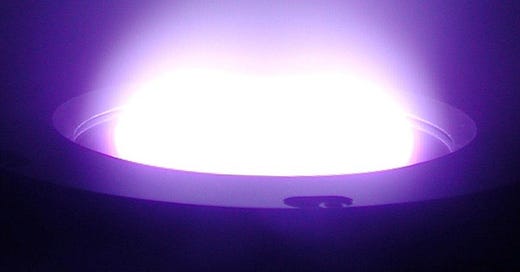
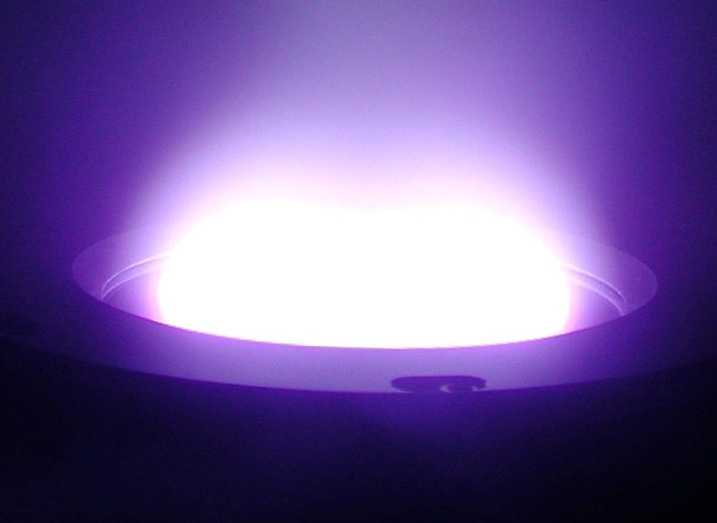
[Seen here: Argon plasma. Each plasma is a different color - Argon is purple!]
Magnetron sputtering uses plasma to bombard a metal target and blast away bits and pieces of the target an atom or two at a time. This is actually exactly the same thing that happens to ion thrusters that use plasma to make their ions - except, for ion thrusters, plasma sputtering is a failure mode, a problem our thruster design specifically avoids by… well… not having a plasma. In a magnetron sputtering system, though, you WANT the bombardment.
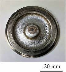
[A 2 inch titanium sputtering target, after about 50 hours of use. Note the indented circle - that’s called the “racetrack”]
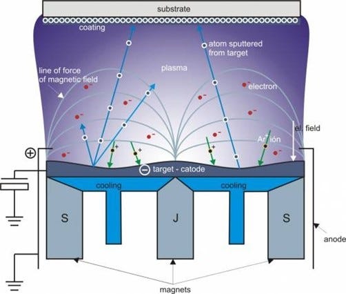
The magnetron sputtering system, in its simplest form, applies a DC field between a conductive target (like the one seen above) and a substrate positioned a short distance away. The target usually has a magnetic field applied to it to guide the formation of plasma at its surface. The DC field accelerates electrons and ions in opposite directions, with the target biased strongly negative and the substrate either grounded or biased slightly positive. So, electrons move toward the substrate, and ions move toward the target. It generally looks like this:
[Note the magnets in center and around the outside of the target mount - those help keep the plasma close to the surface of the target, and are responsible for the racetrack-shaped wear pattern. That’s why they call it “magnetron” sputtering. Also note: The plasma heats up the target, so it’s usually liquid cooled from the back side.]
Gases are fed at low pressure (usually 100 mTorr down to about 5 mTorr) into the space between the target and the substrate and free electrons accelerated between the electrodes slam into the gas molecules, ionizing them (and freeing more electrons in the process). The ions accelerate toward the target and slam into it, which knocks some metal atoms into the space around it. Some of those metal atoms that are knocked free will fly up and land on the substrate, which eventually coats it with whatever material the target is made of.
The gas used is usually argon because it is very inert and won’t usually react with the target material, but you can get a bit fancy and do something called “reactive sputtering” where you mix in oxygen, nitrogen, or other gases, If you do, then the target material reacts with the gas before it reaches the substrate and you can get a different material than you started with - for example, if I have an aluminum target, and I sputter it in a mix of oxygen and argon, it will react with the oxygen in flight, and I will get a coating of Al2O3 (i.e. alumina, or sapphire if it is crystalline) on my substrate. It is typically hard to get these coatings to be perfectly balanced from a chemical perspective - usually there is a little bit of aluminum that makes it to the substrate without reacting, and often a little bit of argon that gets trapped, or a little bit of hydrogen mixed in because there was some water contamination in the chamber. You can get relatively close though.
Now, this works great for conductive metals and for metal-oxides and metal-nitrides made from conductive metals. You can use DC magnetron sputtering with any kind of conductive target, and even use mixed alloys to get some very interesting deposition materials. But, what if you want to coat your substrate with something non-conductive?
Well, the positively charged ions will bombard the target initially if you apply an electric field to an electrode behind it, but the target will trap those charges instead of conducting them away. The target will quickly accumulate a positive charge that neutralizes the negative DC bias, which will cause the plasma to fail, and the process to shut down. Not useful.
To overcome this problem, clever engineers made use of our old friend, the RF electrical signal. By switching at RF frequencies from positive to negative and back again, when a non-conductive target accumulates some ions on one cycle, they are neutralized by electron bombardment on the next cycle. The target thus stays net neutral, and the ions still impact with enough energy to sputter the target and coat the substrate. This approach is a bit more complicated, but significantly increases the flexibility of magnetron sputtering technology.
Spacecraft also run into similar problems of ion implantation and charge buildup in exposed insulating materials, which can lead eventually to arcs, static discharge, electrical failure, or sometimes instrument errors. I’m continuously amazed by the parallels I see between cleanroom techniques and space technology. It shouldn’t be a surprise - physics works the same no matter where you are. But it always surprises me, nonetheless.


